
Single-electron and single-hole transistors represent a fundamental device platform for ultra-low-power charge logic, ultrasensitive charge sensing, and silicon-based spin qubits. By controlling the transport of individual charge carriers through a nanoscale Coulomb island, these devices provide a direct route toward charge-level information processing and quantum-state readout. However, the fabrication of ultrasmall quantum dots bounded by two reliable tunnel barriers remains a major bottleneck. Conventional approaches usually require electron-beam lithography, extreme ultraviolet lithography, pattern-dependent oxidation, or complex gate-defined architectures, which increase fabrication cost and make scalable integration difficult.
To address this challenge, Professor Linwei Yu's group from the School of Electronic Science and Engineering, Nanjing University, in collaboration with Professor Shaoyun Huang's group from Peking University, developed a deterministic step-necking strategy based on the in-plane solid-liquid-solid (IPSLS) growth of silicon nanowires. By guiding catalytic silicon nanowires to grow across closely spaced double steps, the team induced two ultranarrow tunnel constrictions at prescribed positions. These two necked regions flank a central silicon quantum-dot island and naturally form the double-barrier structure required for a single-hole transistor, without relying on high-resolution lithography.In his growth process, indium catalyst droplets drive the lateral crystallization of silicon nanowires along predefined guiding steps. When the droplets encounter sharp convex corners of the double-step structure, the local precursor supply and interfacial force balance are altered, leading to strong necking of the silicon nanowire. As a result, a central island of approximately 50 nm can be isolated by two much narrower constrictions. This self-positioned island-neck geometry provides strong size confinement and enables single-hole transport through a planar silicon nanowire channel.Systematic structural characterization confirmed that the double-step design can reproducibly generate island-neck silicon nanowires. The nanowire diameter was found to shrink at both step corners while becoming thicker in the central island segment, yielding an island-to-neck diameter ratio that can be tuned by controlling the catalyst droplet size. This morphology control is difficult to achieve through conventional top-down etching, because the step-necking process simultaneously reshapes the width and height of the nanowire in three dimensions.The team further fabricated top-gated silicon nanowire single-hole transistors using the optimized island-neck channels. Transport measurements revealed clear Coulomb blockade oscillations at 40 K and well-defined Coulomb diamonds in the charge stability diagram, demonstrating that the central silicon island functions as a single Coulomb-blockaded quantum dot. From Coulomb diamond analysis, the total island capacitance was extracted to be approximately 2.62 aF, corresponding to a charging energy of about 60 meV. This charging energy is much larger than the thermal energy at 40 K, supporting robust single-hole isolation at elevated cryogenic temperature.This work provides a low-cost, scalable, and deterministic route to define tunnel barriers and Coulomb islands directly during silicon nanowire growth. The step-necking approach is expected to contribute to future silicon-based single-charge logic, charge sensors, and spin-qubit devices, and offers a new strategy for constructing quantum-dot structures in planar semiconductor nanowire systems.
Figure Guide
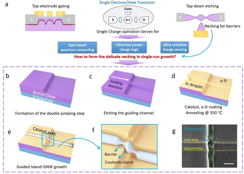
Figure 1. Concept, fabrication strategy, and prescribed formation of step-necked silicon nanowire quantum-dot structures for single-hole transistors.
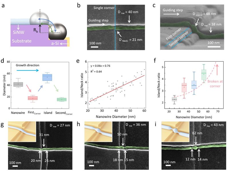
Figure 2. Step-necking growth mechanism and structural characterization of island-neck silicon nanowires. The double-step geometry produces two necked tunnel constrictions and a central silicon island, with the island-to-neck ratio controlled by nanowire diameter and catalyst droplet size.
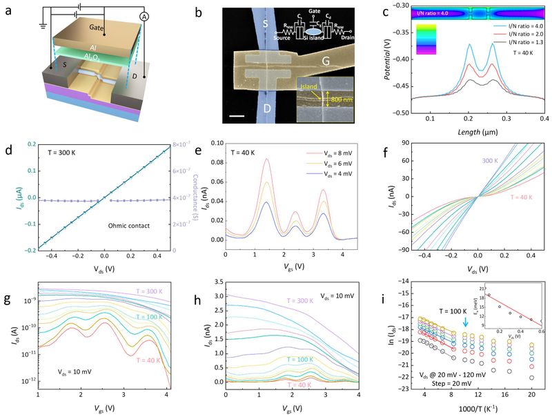
Figure 3. Device structure, electrostatic simulation, and temperature-dependent transport characteristics of the island-neck silicon nanowire single-hole transistor. Coulomb oscillations are observed at 40 K, while simulations reveal a robust double-barrier potential profile.
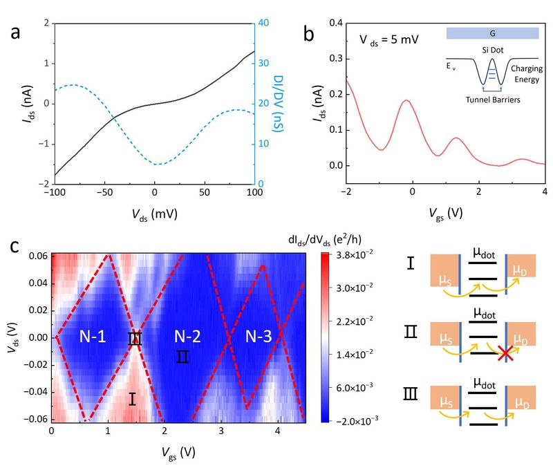
Figure 4. Coulomb blockade characteristics and charge stability diagram of the silicon nanowire single-hole transistor. Pronounced Coulomb blockade regions and Coulomb diamonds demonstrate single-hole transport through the engineered silicon quantum dot.
Recently, this research work was published in ACS Nano under the title "Step-necked tunnel constrictions in Si nanowires enable 40 K quantum-dot single-hole transistors without high-resolution lithography". Zhiyan Hu from the School of Electronic Science and Engineering, Nanjing University. Professor Linwei Yu and Professor Junzhuan Wang from Nanjing University, and Professor Shaoyun Huang from Peking University, are the co-corresponding authors. This work was supported by Professor Kunji Chen, Professor Yi Shi, and Professor Jun Xu from Nanjing University.This work was funded by the National Natural Science Foundation of China for Distinguished Young Scholars, the National Key Research Program of China, and the National Basic Research Program of China. The authors sincerely acknowledge all of the support.
Paper Information:
Step-necked tunnel constrictions in Si nanowires enable 40 K quantum-dot single-hole transistors without high-resolution lithography.
Zhiyan Hu1, Shichang Fan2, Tianyao Wei1, Lei Yan1, Junyang An1, Wei Liao1, Songlin Li1, Shaoyun Huang2*, Junzhuan Wang1*, Linwei Yu1*
Corresponding Authors: Shaoyun Huang, Junzhuan Wang, Linwei Yu
ACS Nano, DOI: 10.1021/acsnano.6c00514(2026)
Previous Related Work:
1. Liao, W. et al. High-Performance Gate-All-Around Field Effect Transistors Based on Orderly Arrays of Catalytic Si Nanowire Channels. Nano-Micro Lett.17, 154 (2025).
2. Wu, L. et al. Step-necking growth of silicon nanowire channels for high performance field effect transistors. Nat. Commun.16, 965 (2025).
3. Liang, L. et al. Extremely Uniform Growth Integration of Stacked Silicon Nanowire Channels for High-Performance Transistors via an Embedded-Precursor-Feeding Strategy. ACS Nano, (2025).
4. An, J. et al. Lithography-free, site-controlled germanium quantum dots in silicon nanowires for single-hole transistors operating up to 50 K. Sci. Adv.12, (2026).
5. An, J. et al. Stable, Step‐Guided Growth of Planar Germanium Nanowires at 200 °C via the In‐Plane Solid‐Liquid‐Solid Mechanism. Adv. Sci., (2025).
6. Xue, Z. et al. Engineering island-chain silicon nanowires via a droplet mediated Plateau-Rayleigh transformation. Nat. Commun.7, (2016).
Research Group Profile:https://ese.nju.edu.cn/ylw
