
Recently, the research team led by Professors Yuan Du and Li Du from Nanjing University has made a major breakthrough in the field of high-speed integrated circuit interconnection. In collaboration with the research team of T-Head (Shanghai) Semiconductor Co., Ltd., the team's relevant research findings, entitledA 47.0Tb/s/mm 112Gb/s/pin PAM4 Single-Ended Transceiver Featuring 4-Aggressor Crosstalk Cancellation and Supply-Noise Tolerance for Short-Reach Memory Interfaces, were presented at the 2026 IEEE International Solid-State Circuits Conference (ISSCC), the top international conference in the field of integrated circuits. This achievement has set a world record for an ultra-high edge bandwidth density of 47.0Tb/s/mm. The related technologies have been applied to the R&D of interfaces for AI computing chiplets and HBM memory chiplets, and the corresponding products have been featured on CCTV News, providing core technical support for domestic AI chips to benchmark international advanced levels.
Figure 1 The research team led by Professors Yuan Du and Li Du from the School of Electronic Science and Engineering, Nanjing University, presenting their paper at ISSCC 2026
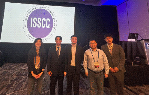
Figure 2 Group photo of the session chair of the Memory Interface Track and the presenters at ISSCC 2026
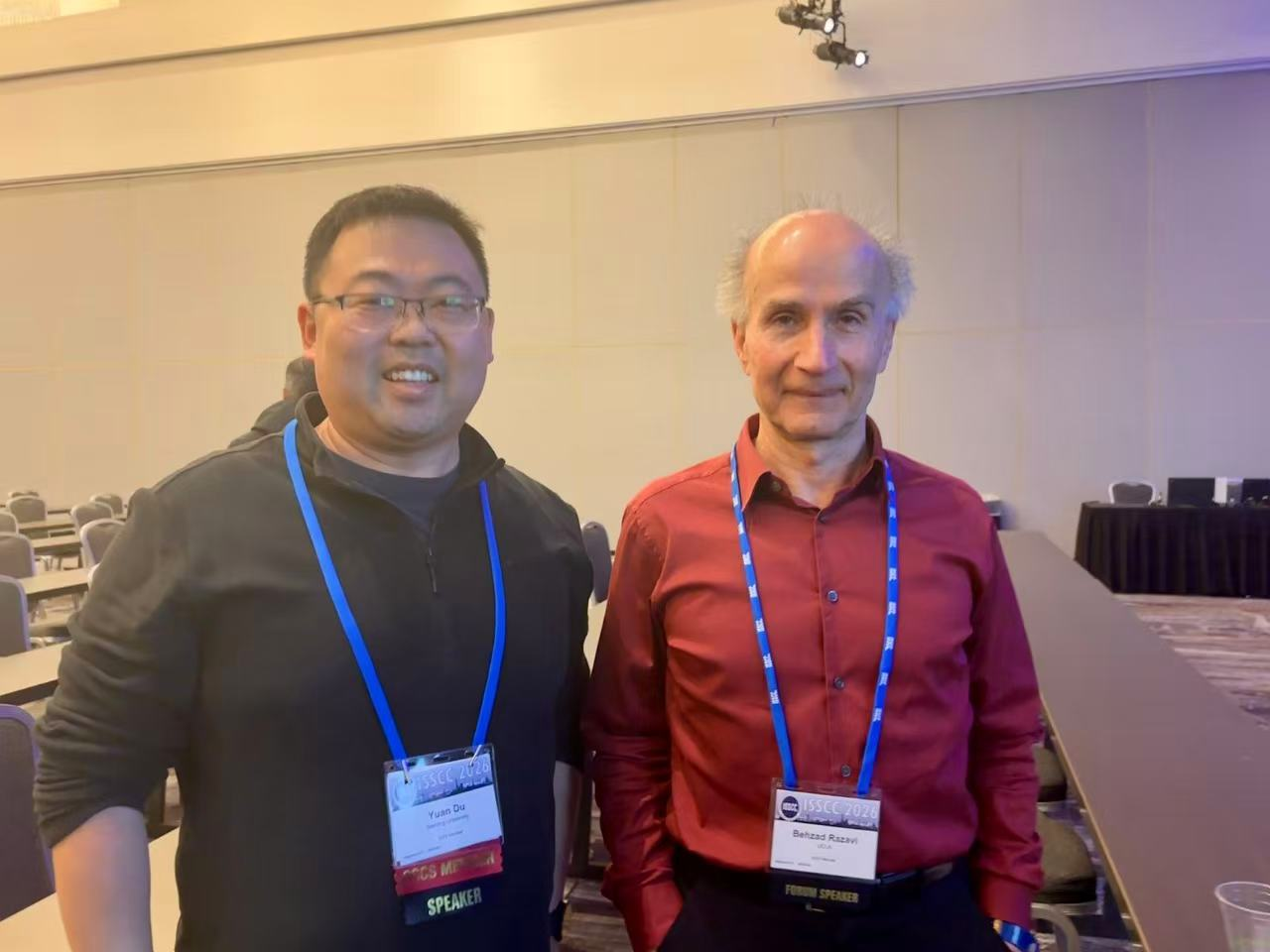
Figure 3 Behzad Razavi, a world-renowned UCLA professor and preeminent authority in analog/RF IC design, witnessed Nanjing University’s research debut at ISSCC 2026
With the explosive development of high-performance computing and artificial intelligence technologies, the demand for high-bandwidth and high-density transmission in short-reach chiplet interfaces such as HBM and UCIe has surged, and single-ended (SE) signal transmission has become the mainstream solution for achieving high-bandwidth I/O density. However, in ultra-high-speed transmission scenarios, the industry is confronted with three severe challenges: power consumption, crosstalk, and supply noise. High-order modulated single-ended signals are extremely sensitive to various types of noise interference. Traditional solutions either only support low-rate transmission or fail to balance power consumption and signal integrity, making it difficult to adapt to high-density application scenarios of multi-layer interposers. This has become a core bottleneck restricting the development of high-speed interconnection technologies.
To address these industry pain points, the research team designed a five-lane 112Gb/s/pin PAM4 single-ended transceiver integrated with 4-aggressor crosstalk cancellation and supply-noise tolerance technologies based on the 28nm CMOS process (Figure 4). This design overcomes the signal integrity challenges of high-density short-reach memory interfaces, with its core indicators reaching the international leading level. The core innovations and contributions of the chip are mainly reflected in three aspects:
Low-power front-end design balancing energy efficiency and signal compensation: A low-power triple-equalization driver and a resistive feedback amplifier termination scheme were developed, and a lightweight multi-frequency equalizer was designed for the characteristics of short-reach channels. This design achieves a 9.1dB improvement in signal loss compensation with an overall power consumption of only 3.8mW, significantly enhancing energy efficiency.
4-aggressor crosstalk cancellation solving high-density crosstalk challenges:A pioneering 4-aggressor shape-fitting crosstalk cancellation technology was proposed. Through delay matching and pulse waveform fitting, the completely closed eye diagram of the 112Gb/s PAM4 signal is improved to an effective eye diagram with an opening of more than 160mUI × 40mV at a bit error rate (BER) of <10⁻⁹, realizing effective compensation for four crosstalk aggressors and providing reliable support for ultra-high-speed signals in ultra-high-density scenarios.
Supply-noise-tolerant clock network improving system robustness:A global clock distribution network based on transmission lines combined with a local clock network with supply-noise compensation was designed, which greatly reduces signal jitter caused by supply noise. Under a 100mV supply noise, the fluctuation of the signal eye width is limited to within 5%, significantly improving the system's tolerance to supply noise.
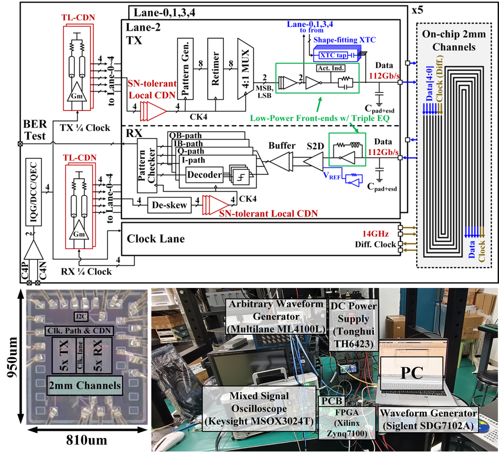
Figure 4 Architecture and testing of the prototype chip
Test results show that the chip achieves effective transmission at 5×112Gb/s with a BER of less than 10⁻⁹, reaching the international leading bandwidth density of 47.0Tb/s/mm and energy efficiency of 0.52pJ/b. It can effectively cope with harsh crosstalk and supply noise environments, with signal integrity and transmission reliability significantly outperforming traditional solutions (Figure 5).
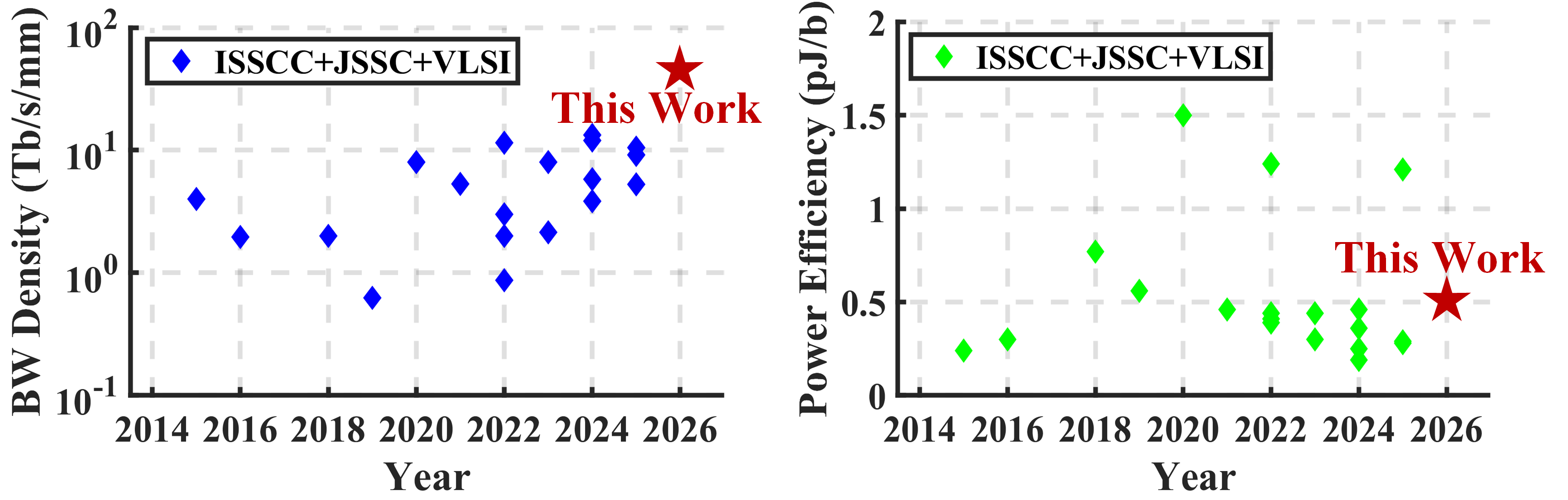
Figure 5 The bandwidth density and energy efficiency reaching the international leading level
Qian Liu, a 2024 PhD candidate at Nanjing University, is the first author of the paper. This research was supported by the National Key R&D Program of China and the Jiangsu Provincial Key R&D Program. It also received funding and technical support from T-Head (Shanghai) Semiconductor Co., Ltd., serving as an outstanding example of Nanjing University deepening industry-university collaborative innovation and promoting the translation and commercialization of scientific research achievements.
Paper link:http://ieeexplore.ieee.org/document/11408977
