Recently, the research team led by Professor Yi Shi and Associate Professor Hao Qiu from the School of Electronic Science and Engineering at Nanjing University has achieved a significant breakthrough in wireless power transfer (WPT) technology. The results were published online on April 16 in IEEE Journal of Solid-State Circuits (JSSC), under the title: “A 6.78-MHz single-stage regulating rectifier with dual outputs simultaneously charged in a half cycle achieving 92.2% efficiency and 131 mW Output Power.”
Invasive brain-computer interfaces (BCIs) require long-term implantation within the human body. Constrained by biosafety standards and sealed physiological environments, these devices cannot utilize physical wires for power delivery and must instead rely on wireless power transfer. Moreover, their highly compact packaging severely limits thermal dissipation capabilities. If heat generated from power loss is not effectively managed, it can degrade circuit performance, trigger device failure, or even cause thermal damage to surrounding biological tissues. Consequently, maximizing power conversion efficiency (PCE) and minimizing intrinsic heat dissipation have become critical design objectives for implantable power management circuits.
Against this backdrop, single-stage dual-output regulating rectification has emerged as a promising solution, offering an optimal balance between miniaturization and high efficiency. It is widely regarded as an ideal approach for enabling long-term, safe power delivery to invasive implants and has attracted increasing academic attention. However, conventional implementations face three primary challenges: (1) traditional architectures typically employ time-multiplexed operation or half-wave rectification, which restricts the effective charging window and limits both output power and conversion efficiency; (2) achieving independent and precise voltage regulation across multiple outputs remains difficult, with existing topologies often suffering from excessive voltage ripple due to cross-coupling or mismatched hysteresis control; and (3) widespread reliance on PMOS-based active rectifiers introduces substantial conduction and switching losses.
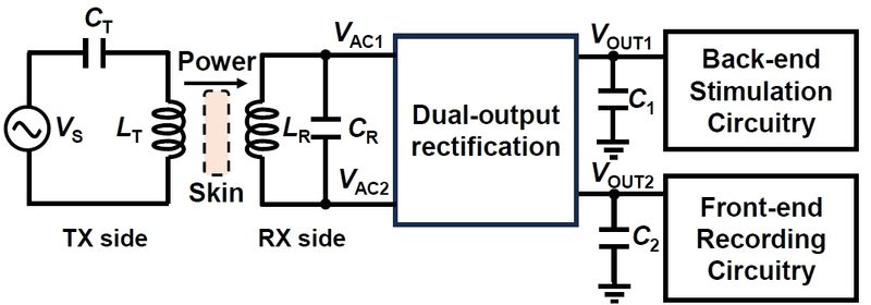
Fig. 1. Schematic of the wireless power transfer system for an invasive BCI.
To address these limitations, the research team proposes a novel high-efficiency single-stage dual-output regulating rectifier topology. Unlike conventional designs, this architecture enables simultaneous charging of both outputs within a single half-cycle, overcoming the limitations of time-multiplexed operation and significantly enhancing load power delivery, supply voltage quality, and overall energy conversion efficiency. Furthermore, an innovative charge allocation scheme is introduced to mitigate performance degradation caused by load imbalance between the dual outputs. By adaptively optimizing charge distribution across multiple output nodes, the design effectively widens the rated output current range and substantially improves circuit stability and adaptability under dynamic load conditions.
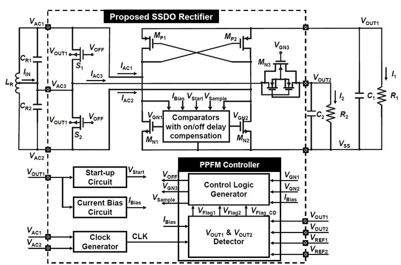
Fig. 2. Schematic of the proposed single-stage dual-output regulating rectifier.
The proposed rectifier chip was fabricated using a standard 0.18-μm CMOS process. Measurement results demonstrate a peak power conversion efficiency of 92.2% and a peak output power of 131 mW under steady-state operation. The dual output voltages are tightly regulated at 3.3 V and 1.6 V, with maximum ripple voltages maintained within 50 mV and 75 mV, respectively. During large load transient steps (×15), the circuit achieves fast dynamic response while effectively suppressing cross-regulation interference between the two outputs. Several key performance metrics set new international records for comparable state-of-the-art designs.
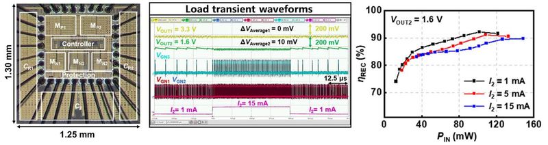
Fig. 3. Photo of the rectifier chip, along with measured load transient waveforms and efficiency curves.
Quanrong Zhuang, a Ph.D. student at the School of Electronic Science and Engineering, Nanjing University, is the first author of the paper. Associate professor Qiu Hao and professor Shi Yi are the co-corresponding authors. Dr. Zhang Xin from the IBM Thomas J. Watson Research Center provided guidance for this work. The research was supported by the National Natural Science Foundation of China (including key projects, the first batch of overseas outstanding young talents projects, general projects, and innovative research group projects), as well as the Ministry of Education Engineering Center for Optoelectronic Materials and Chip Technology and the Center for Future Intelligent Chips.
Link to the paper: https://ieeexplore.ieee.org/document/11482605