Recently, Prof. Rong Zhang and Prof. Xuefeng Wang’steam fromNanjingUniversity has achieved an important breakthrough in the field of phase-engineering topological quantum materials, in close collaboration with the groups from University of Chinese Academy of Sciences, Institute of Metal Research of the Chinese Academy of Sciences, Dalian University of Technology, and other institutions. They directly observed the thermally driven large-area atomic reconstruction from palladium ditelluride (PdTe2) to palladium telluride (PdTe). Both materials possess topological and superconducting properties. Combining in-situ electron microscopy analysis and atomic-scale molecular dynamics simulations, they also clearly elucidated the intrinsic mechanism underlying this large-area phase transition. This study not only provides a universal strategy for the large-scale fabrication of transition metal chalcogenides, but also offers new insights into understanding the modulation of spin splitting of energy bands by symmetry breaking in heterojunctions. Meanwhile, it lays a solid material foundation for potential applications in post-Moore-era chip interconnection, low-power spintronic chips, new terahertz sources, photodetection, quantum sensing, and quantum computing. This work entitled “Large-area non-stoichiometric phase transition in transition metal chalcogenide films” was published online in Nature Materials on January 16, 2026.
Topological quantum materials belong to a vital class of next-generation spintronic materials and have topologically protected electronic states and low-dissipation transport characteristics. Currently, a key challenge hindering their practical applications lies at the high-quality controllable synthesis of large-area thin films and their heterostructures. Phase engineering adopts an unconventional material fabrication paradigm by precisely modulating the crystalline structural phases. It enables the directional design of material properties and functions. This approach not only breaks through the limitations imposed by traditional material categories, but also allows for the stable regulation of the crystalline phase composition, distribution and interfacial properties of thin films, thereby providing a brand-new solution for fabricating large-area, high-quality and target-function-oriented topological materials. Nevertheless, phase engineering for topological materials is generally sophisticated, and precise modulation has remained confronted with numerous challenges. Although remarkable progress has been achieved in static characterization and observation based on phase engineering, it is still a crucial bottleneck for realizing large-area controllable phase transitions and device applications to unravel the phase transition dynamics and the accompanying atomic-scale reconstruction mechanisms on the atomic scale.
To address the aforementioned challenges, the research team firstly fabricated centimeter-scale epitaxial PdTe2 thin films on sapphire substrates by leveraging a custom-made pulsed laser deposition (PLD) technique, with in-situ monitoring via reflection high-energy electron diffraction (RHEED). Subsequently, using scanning transmission electron microscopy (STEM) equipped with in-situ heating capabilities, the team directly visualized the atomic-scale reconstruction dynamics of the phase transition from PdTe2 to PdTe during thermal treatment on the atomic scale. Combined with machine learning molecular dynamics simulations, they systematically uncovered the coherent mechanism, which includes thermally driven vacancy generation, Pd-Te bond reconstruction, and the subsequent collapse and closing of van der Waals gap. The as-prepared PdTe thin films exhibit excellent superconducting properties, with a superconducting transition temperature comparable to that of single-crystal bulk materials. Moreover, the formed atomically sharp PdTe2/PdTe heterointerfaces with the intrinsic lattice mismatch demonstrate the giant helicity-dependent terahertz wave emission based on spin photocurrents.
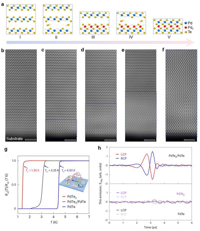
Figure:a-f,Schematic of thermally driven atomic reconstruction in PdTe2 andIn situ STEM observations of phase transition from PdTe2 to PdTe under heating. Thescale bar is 2nm.g,h,Temperature dependence of the normalized resistanceand helicity-dependent terahertzemissionfor thinfilms with differentPd-Tephases.
Furthermore, the strategy for thermally driven large-area non-stoichiometric phase transitions can be extended to other transition metal chalcogenide systems such as PtTe2, holding promise for developing a promising intelligent material platform for non-stoichiometric phase transitions. This study breaks through the visualization technology of large-area atomic-scale reconstruction phase transitions. It not only provides a universal method for the large-area fabrication of transition metal chalcogenide films and their heterostructures, but also drives their potential applications in forefront fields including advanced terahertz sources, low-power spintronic chips, chip interconnection, topological quantum devices, and superconducting quantum computing.
The corresponding authors of this paper are Prof. Rong Zhang, Prof. Xuefeng Wang from the School of Electronic Science and Engineering at Nanjing University, Prof. Wu Zhou from the University of Chinese Academy of Sciences, Prof. Teng Yang from the Institute of Metal Research of CAS, and Prof. Junfeng Gao from Dalian University of Technology. The joint first authors are Dr. Zhongqiang Chen (currently postdoctoral researcher at the School of Electronic Science and Engineering at Nanjing University), Dr. Jin-an Shi, Dr. Jianqi Huang and Dr. Yuan Chang. The collaborative team also includes Profs. Yi Shi, Xinran Wang, Baobing Jin, Fengqi Song, Yongbing Xu, Liang He, Yufeng Hao, Xiaoxiang Xi, and Feng Ding. This work was financially supported by the National Natural Science Foundation of China (NSFC), the National Key R&D Program of China, and the Innovation Program for Quantum Science and Technology of China. Additionally, the research has received substantial technical support from the following excellent platforms: Nanjing Institute of Atomic Scale Manufacturing, State Key Laboratory of Spintronics, Jiangsu Provincial Key Laboratory of Third Generation Semiconductors and High Energy Efficiency Devices, Collaborative Innovation Center of Advanced Microstructures, and the Electron Microscopy Center of the University of Chinese Academy of Sciences.
Paper link: https://www.nature.com/articles/s41563-025-02471-9